


MAY 2009: While using a smart phone that performs all the scintillating digital magic earlier done by a computer, have you ever fancied what triggers the wonder? Or what helped these devices shrink their size while enduring power and performance?
Well, the wizard here is called surface-mount components—said to be the lifeline of surface-mount technology. Any electronic device—from LCD TVs to the latest small mobile phones—is today packed with these tiny devices. These devices help manufacturers pack more electronic components in a much smaller space while enabling more functionality.

SMT vs through-hole technology
The evolution of surface-mount technology dates back to the 1960s. However, this technology caught the fancy of users across the globe only in the 1980s. (For more details, see April 2008 issue of EFY.) Unlike its popular counterpart through-hole technology, components in SMT are directly mounted onto a printed circuit board (PCB). In through-hole, pins are inserted into drilled holes on a PCB.
SMT components have small metallic end caps which are directly soldered onto the PCB surface. This technology reduces the package size and improves functionality to a great extent on the same board-area. SMT places components on both sides of the PCB, which helps to reduce time in assembling the components. Placing components on both sides of the board also allows much higher circuit densities.
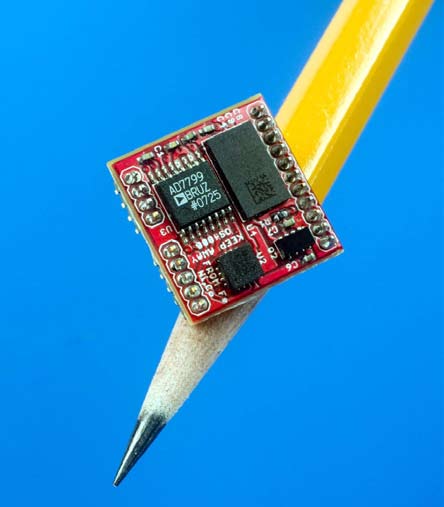
Surface-mount devices are very small and thin, compared to through-hole. Specifically speaking, these are one-quarter to one-tenth the size and weight, and one-half to one-quarter the cost of equivalent through-hole parts. This allows lower resistance and inductance at the connection, leading to better performance for high-frequency parts.
SMT components
Basically, SMT components come in two forms—passive and active. Passive SMT components include resistors and capacitors, while active components include diodes, transistors and integrated circuits.
In electronics industry, especially in the SMT segment, technologies are congregating to increase efficiency while keeping costs low. “Passive and active components are becoming so small today that these are barely visible to the human eye. Companies are integrating more functions into these tiny devices, helping fine-pitch these components,” says Prasad Chandrakant Gurjal, managing partner, Drive Technologies.
The prospect of reduced operational cost and time, as well as improved quality, is driving investment into research and development. Packaging style is improving so that components can be made as small as possible. The industry is reducing package dimensions of surface-mount device (SMD) resistors while maintaining fixed electrical performance characteristics of leaded devices. Size and weight are getting reduced because of lower voltages and higher speeds.
General trends
The growing demand for miniaturisation of consumer electronics has helped to reduce the size of passive SMT components. The 1210 and 1206 component sizes of the 1980s changed to 0402 and 0201 in the late 1990s.
“Today, the new and emerging size of 01005 is in demand, while 0603 and 0402 components have been in vogue in the recent years. These component sizes have been run in high-volume applications at very high yields for long time,” says S.K. Jain, CEO and MD, Sumitron Exports.
The new-generation wireless products require more functionality in less space, with lower weight, less power consumption and at higher frequencies. This is driving the use of smaller passives for system-in-package (SIP) modules. Lately, 0201 components have been used in such wireless applications as mobile phones and bluetooth devices. Capacitor and resistor manufacturers are now offering low-volume quantities of 01005 components and semiconductor companies, and electronics assembly manufacturers are gearing up to develop, and qualify, manufacturing processes, assemblies and components for their respective applications.
Design and packaging
With the growing complexity of components, interconnection density in the packaging is increasing. At the same time, there has been a large reduction in board space usage, and an increase in input/output (I/O) capacities. Companies are dreaming big here. The ultimate package is likely to perform all functions on a single integrated circuit (IC). Immense research is going on to improve packages such as ball-grid arrays (BGAs) and chip-scale packages (CSPs).
[stextbox id=”info”]Size is still being reduced. Previously, bigger SMD packages like SOT89 were widely used. Now SOT 23 is commonly available.[/stextbox]
The new series of consumer products are currently using CSP-size components. To attain the functionality and density of bare die assembly, new-generation devices have been introduced by the packaging industry. CSPs are 1.2 or 1.5 times larger than the perimeter or the area of the bare die. These devices assume the stress of miniaturisation while retaining the benefits of conventional IC packages. With growth in the CSP technology, the devices could be reduced to almost the size of the integrated circuit die itself.
The other package is in the form of a reduced-scale BGA, either in a partially or fully populated I/O condition.
