


DECEMBER 2011: Surface-mount technology (SMT) is one of the key factors for the shrinking electronics system-level packaging. The key drivers for SMT in India are the use of surface-mount devices (SMDs) in products developed indigenously by the Indian companies in the private as well as government sector, and the sourcing strategies of global electronics leaders and original equipment manufacturers (OEMs) to have their own manufacturing set-ups in India, or outsourcing the manufacturing to Indian or global contract electronic manufacturers (CEMs).
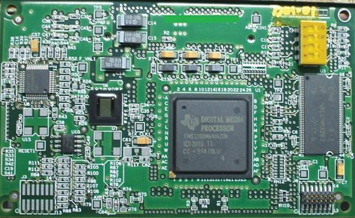
With the electronics packaging being an ever-evolving field, and the focus on shrinking the size and having more packaging capability within the same or lesser real estate, component packaging has shrunk as well. Due to the condensed component structure, the component fan-out has increased multi-fold. To cater to this increased fan-out, printed circuit boards (PCBs) have moved from the conventional two-sided boards to multi-layer boards, with many manufacturers choosing high-density interconnect (HDI) methods for their designs.
PCBs, components and systems
Though SMD components manufacturing in India is not in line with the global trends, some manufacturing is taking place. Majority of the components used for board manufacturing are still sourced from abroad.

However, interconnect structure and PCB fabrication are moving quite closely with the global trends. A few PCB fabrication houses are capable of fabricating advance-level boards using HDI techniques. Most of the globally accepted low-loss laminate materials are available in India for the PCBs. Various metallic and organic surface finishes are also available. The cumulative result is advanced PCBs catering to both leaded and lead-free processes in India.
Areas of growth for PCB manufacturing include flexible PCBs, metal-clad PCBs and PCBs with embedded discretes. Flexible PCB manufacturing that has 2D flexural capability can be seen widely in India, though 3D flexural capability is yet to catch up. Metal-clad PCBs manufactured in India are widely being used for LED applications helping meet mechanical design constraints. PCBs by Indian OEMs with various embedded components are under prototype qualification stages. Especially for consumer electronics, these are set to see wide usage in the next few quarters.
Though there has been commendable progress within PCB manufacturing, this segment is still at a nascent stage in India. The upward trend still stays within very few Indian and global PCB fabrication houses who have their manufacturing in India. Most of the PCB fabrication houses still lag behind and need to have the understanding of the international standards and customer expectations. This is a major reason for increased cost of the boards fabricated in India, resulting in high dependency on PCBs from abroad.
Solder and associated material
SMT is driving the advances in solder materials, as the requirements for finepitch printing and reliable solder joint with minimal solder volume become a challenge. Smelting houses in India have been the main source of raw solder materials within the country for a long time.
With leading global solder consumable manufacturers sourcing raw materials from India, the manufacturing processes for smelting houses now meet world-class levels. Also, a few global solder consumable manufacturers have set up offices in India offering high-quality support, which, in turn, has raised the support requirements from Indian solder consumable manufacturers. This finally benefits the customers, specifically the CEMs who normally interact with more than one supplier.
Halogen-free requirement is another upcoming area of work. With this as a regulation, the challenges faced by the CEMs in India are very similar to the ones faced globally. This informa-tion is being used constructively by the solder material manufacturers.
Flux is now available in various forms—liquid, paste or solid—and various corrosion levels. This has significantly helped in soldering components of various types, which have various flux requirements within the same board, or which require more than one type of solder. One good example is customised components with castellation and thermal pad on the bottom. In this case, flux in paste form is used as part of the solder paste and additional solid flux is used in castellation.
PCB surface finishes and the chemicals used also have a heavy influence on the direction in which SMT moves. OEMs and subsequently the PCB fabricators are moving away from the metallic (hot-air solder leveling) and electroplated finishes (electroless nickel immersion gold and electroless nickel electroless palladium immersion gold) towards organic finishes (organic solderabilty preservatives (OSPs)).
Major challenges with the organic surface finish are the fidelity of contact during the test of the PCB assembly and traces of OSP left behind. Advances in this area with conductive solder finishes (which is under qualification with a few Indian PCB fabricators) will help mitigate this challenge and streamline the use of organic surface finishes.
