Various research projects for SMT are undertaken by Indian academic institutions in partnership with the industry. The primary focus is on alternative lead-free solder alloys with soldering profile similar to legacy Sn63/Pb37 (tin-lead) alloy and also alternative to the widely used SAC (An-Ag-Cu) alloys. PCB surface-finish defects elimination in the wet process is another primary research area.
Equipment
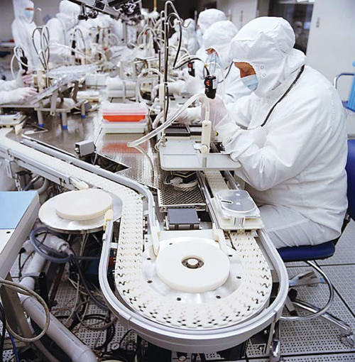
Majority of the equipment used for electronics manufacturing, cleaning and inspection are imported. All the major equipment manufacturers either have direct presence or authorised dealers. Majority of the equipment vendors excel in post-installation and annual maintenance support. With most high-speed electronics equipment and advanced soldering equipment available, advanced manufacturing using six-sigma approach and meeting stringent goals is being done in India.
Rework equipment for advanced packages are another focus area. With several players working in the prototyping and rework segment, use of precision rework equipment—both automated and manual—has grown significantly.

Automated board handling is another area of high growth. These subsidiary equipment used along with the main assembly equipment help increase manufacturing efficiency and process yields. With automated board handling equipment being used in the industry, process defects introduced due to manual handling—like wrong board orientation, ionic cleanliness requirements, etc—are almost eliminated.
Tooling
Customised tooling has always been a requirement for electronics manufacturing. As miniaturised component usage increases manifold, new challenges are being faced by tool vendors. The first customised tool used in electronics manufacturing is the stencil. IPC-7095 and different stencil design patterns and requirements are already known to the stencil manufacturers in India. In addition to these, various types of step-etched (level-etched) stencils are now in practice.
As more and more OEMs choose OSP as their preferred surface finish and move away from dual surface fin-ish designs, additional solder deposition challenges are faced by the stencil manufacturers—for example, requirements of less than 0.1016 millimetre (4 mil) of overall solder deposition to allow for both EMI suppression effect as well as meet the stringent mechanical constraints. As SMD component usage far surpasses the use of through-hole components, specialised stencil designs help use intrusive solder techniques as the preferred method for soldering through-hole components, thereby reducing manufacturing steps significantly.
PCB assemblies that use adhesives for SMD component assembly require specialised wave-soldering pallets for soldering of component termination post-SMD assembly. Wave-soldering pallets meeting world-class standards are now available from Indian tool manufacturers.
With SMD density increasing manifold, the number of test-points need to be reduced to meet the real-estate requirement. In-circuit test (ICT) still remains the preferred test and programming stage for PCB assemblies. Circuit test-beds and fixtures development and manufacturing are the areas that need to scale up.
With various OEM service support centres based in India, rework fixtures like localised stencils and ball-grid array (BGA) re-balling fixtures have seen phenomenal growth. These along with specialised requirement are available in India for quick turnaround times. Also, test fixtures for prototype requirements are readily available for introducing new products.
Facilities
Facilities in conformance with ANSI/ESD S20.20 certification are one of the primary requirements for electronics manufacturing. With every CEM and OEM seeking to establish electrostatic discharge (ESD) protection in its facilities, higher-level segregation based on the ESD sensitivity of the components being handled is used. Also, within the same ESD-protected area, smaller areas with specialised facility requirements are established to handle higher-sensitivity components (like
Lead-free manufacturing is another driver for resource requirement. Special requirements like nitrogen for high-temperature lead-free assembly introduce requirements for new facilities.
Electronics manufacturing
Unlike PCB fabrication, electronics manufacturing is setting its own global trends. Key driver in this segment is the setting up of facilities by global consumer electronics giants in India.
The push to Indian R&D companies to source the boards from within the country provides enough challenge for the Indian CEMs. Further, the outsourcing strategy of global giants has helped replicate the best practices in manufacturing processes. Component package like 0402 is commonly used to increase package-on-package (PoP) density. Also, larger BGA packages with pitch less than 0.5 mm and dimensions up to 60 mm on the sides are being used for system-on-chips and application-specific integrated circuits. These packages put forth the challenge of higher manufacturing process yields to meet the yield fall-out of these components.
[stextbox id=”info” caption=”Technological advancements in SMT machines”]
The SMT equipment market is witnessing major technological innovations. Growing sophistication and the shrinking size of electronic gadgets is fuelling these advancements. Recent demand within the industry has been for high-precision complex boards and assemblies. At the same time, there is a constant pressure to improve the quality of the goods produced, aiming for zero defects. To be able to manage this, manufacturers need to have the right SMT equipment, which will enable fast, flexible and perfect production of PCBs.