Less power consumption and more efficiency offered by GaAs wafers are attracting the market players to adopt them, thereby increasing the demand for GaAs wafers. Previously, the optoelectronic devices were broadly used in short-range optical communications and computer peripherals but now these are in demand for some emerging applications such as lidar, augmented reality, and face recognition as well.
The recent global shortage of semiconductor chips is playing havoc with the production of electronics goods including white goods and automobiles, which now use lots of these components. The demand has surged far beyond production, which got reduced due to lockdowns and other issues due to Covid-19 all over the world.
With the increasing demand and low supply of electronic basic material such as silicon wafers, scientists, engineers, and manufacturers dealing with electronics industry are always on the lookout for substitute material. Gallium in its combinations as gallium nitride (GaN) and gallium arsenide (GaAs) has emerged as a strong candidate, even if not a replacement for silicon, to at least supplement its shortage with more diverse applications in electronics industry.
Energy savings have become the buzz word in every sphere of our life due to our heavy dependence on energy, its bad environmental effects as well as the depleting resources. Electronic devices as an integral part of our present-day lifestyle can also be a major source of energy savings. But a significant amount of electric energy is being lost during power electronics processes, thus limiting both power efficiency and reliability of electrical and mechanical systems.

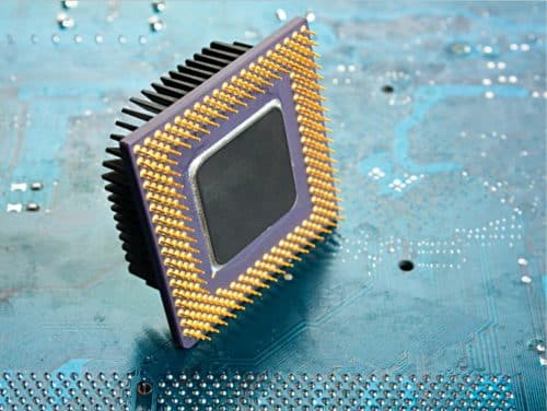
Currently, the three semiconductor materials being used in power electronics are silicon (Si), silicon carbide (SiC), and gallium nitride (GaN). Among these, silicon does not perform well in higher energy density and temperature conditions, and SiC and GaN cannot be used for higher currents and are often too expensive. Therefore, gallium arsenide (GaAs) (see Fig. 1) is widely used in microelectronics due to its suitability for high frequency and temperature, but not for controlling and converting electrical energy.
Science of GaAs
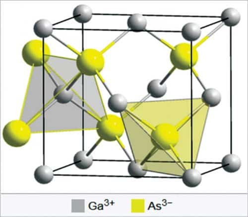
GaAs is a group III-V direct band gap semiconductor having a zinc blende crystal structure. Since GaAs is a compound, each gallium atom in the structure is surrounded by arsenic atoms, and similarly gallium atoms surround each arsenic atom in the structure as shown in Fig. 2 of unit cell structure. Three valence electrons of gallium atoms share with five valence electrons of arsenic atoms. In this way, each of the GaAs atoms gets eight electrons in its outermost shell.
The covalent bonds between arsenic and gallium atoms in a gallium arsenide compound are strong bonds, still it is possible to break the bonds, if sufficient energy is applied externally. Due to the breaking of covalent bonds between arsenic and gallium, electrons come out from the lattice structure of the GaAs compounds. An electron on its separation from the covalent bond leaves a vacancy behind it in the bond. The separated electrons from the bonds are free to move anywhere in the lattice and are referred to as free electrons. Similarly, the vacancies created in the bonds are referred to as holes, and both free electrons and holes are called free charge carriers.
The energy gap between valence band and conduction band in GaAs is 1.43eV, which is the largest band gap as compared to other common semiconductors. Among the three most popular semiconductor materials, the use of GaAs is growing. Because of very high speed operating characteristics, low reverse saturation currents, excellent temperature sensitivities, and high breakdown voltages associated with GaAs wafers, nowadays, the use of GaAs in place silicon has gained ground in manufacturing very large scale integrated circuits. With all these advantages, GaAs is also being widely used in other different optoelectronics applications like LEDs, solar cells, and photodetector devices.

Electron mobility, single junction band-gap, higher efficiency, heat and moisture resistance, and superior flexibility are the five distinct advantages of GaAs, which are improving the acceptance of GaAs wafers in the semiconductor industry. Liquid encapsulation Czochralski (LEC) and vertical gradient freeze (VGF) are two popular methods which are improving the production of GaAs wafers with high uniformity of electrical properties and excellent surface quality.
Unique applications and opportunities
The performance of high-speed semiconductor devices, which almost drive the present-day digital computers, electronic systems for digital signal processing, telecommunication systems, and optoelectronics are undistinguishably linked to the unique physical and electrical properties offered by GaAs. Once viewed as a simple alternative to silicon, gallium arsenide has emerged as an irreplaceable material in component fabrication in leading high-tech industries.
Moreover, the increasing expertise with the fabrication methods, operating principles, device models, novel device designs, the material properties, and physics of GaAs is so integral to this success. GaAs high-speed devices provide a comprehensive and state-of-the-science look. Gallium arsenide eventually has emerged as the favourite material for high-frequency applications due to the high carrier mobility compared with silicon devices.
Wide energy band gap makes pure GaAs highly resistive and, combined with a high dielectric constant, this property makes GaAs a very good substrate for integrated circuits. This provides natural isolation between devices and circuits with GaAs, unlike silicon. This advantage has made it an ideal material in monolithic microwave integrated circuits (MMICs). GaAs devices are particularly useful in very high speed computer circuits and at microwave frequencies above 4GHz in discrete components or microwave monolithic integrated circuits (MMICs).
GaAs based microwave devices have found extensive use in consumer applications as well in sophisticated warfare electronics. The use of GaAs in transistors and integrated circuits for space and military applications has greatly expanded over the past few years.
The unique property of gallium arsenide is its ability to turn electricity into light. Thus, GaAs also exhibits relevant optical properties and finds extensive applications in optoelectronics including LEDs, laser diodes, solar cells, optical windows, and GaAs diodes to detect X-rays. Several solar car models are coming that make use of GaAs in solar arrays.
The main reasons for the exploitation of this semiconductor are that GaAs devices can operate at higher frequencies and have greater radiation hardness than their silicon counterparts. GaAs applications are growing in different fields and it is being used in the manufacture of devices such as microwave frequency and monolithic microwave integrated circuits, infrared LEDs, laser diodes, solar cells, and optical windows. GaAs is also often used as a substrate material for the epitaxial growth of other III-V group semiconductors like indium gallium arsenide and aluminium gallium arsenide. GaAs has been used for various transistor types including the following:
- Metal semiconductor field-effect transistor (MESFET)
- High-electron-mobility transistor (HEMT)
- Junction field-effect transistor (JFET)
- Heterojunction bipolar transistor (HBT)
- Metal oxide semiconductor field-effect transistor (MOSFET)
The superior properties of GaAs compared to silicon, such as higher saturated electron velocity and higher electron mobility, allow GaAs transistors to function at higher frequencies. Due to its wider energy band gap, GaAs devices are relatively insensitive to overheating. As a result of higher carrier motilities and lower resistive device parasitics, they also tend to create less noise (disturbance in an electrical signal) in electronic circuits than silicon devices, especially at high frequencies. These superior properties are compelling scientists, engineers, and manufacturers to think about the use of GaAs circuitry in mobile phones, satellite communications, microwave point-to-point links, and higher frequency radar systems. Besides, GaAs is also being used to manufacture Gunn diodes for the generation of microwaves.
Next-generation GaAs semiconductors and devices promise to create a huge demand, not totally replacing the existing semiconductor market, but ultimately making a huge dent in it. Due to the mounting limitations with the use of silicon, a market of worth $500 billion dollars in 2020 is looking towards the ability to replace silicon semiconductors with more suitable semiconductors. The GaAs wafers/substrates are next-generation technology as they operate faster than the silicon semiconductors. Thus, GaAs represents the next generation of semiconductor chips, which can do things that the silicon chips cannot do.
Next-generation GaAs support the signal speed which is needed to implement 5G supported Internet of Things (IoT). Therefore, the potential for the next-generation GaAs wafers is overwhelming with the overall semiconductor market likely to surpass $20 trillion by 2026. Once world economies appreciate these developments, GaAs semiconductor markets are expected to really take off.
GaAs is a direct band-gap semiconductor with a zinc blende crystal structure and can be used for sensing (3D sensing for consumer electronics and electric vehicles). Its application in radars and for lasers is common. Further, the benefits of using GaAs in devices derive in part from the characteristic that GaAs generates less noise than most other types of semiconductor components and, as a result, it is useful in weak-signal amplification applications. Due to the benefits related to generating less noise, GaAs is again a suitable replacement for silicon in the manufacture of linear and digital integrated circuits.
Design challenges
The environment, health, and safety aspects of GaAs sources (such as trimethylgallium and arsine) and industrial hygiene monitoring studies of metalorganic precursors designate gallium arsenide as a carcinogen.
Another biggest drawback with GaAs is the high cost of a single-crystal GaAs substrate, which has been a barrier to volume manufacturing.
Further, just as in silicon devices, the seeds of GaAs contact reliability problems are often planted during processing and contribute to reducing contact quality, conducting projections that threaten to short the formed GaAs layer.
The application of ion implantation for the fabrication of GaAs devices has not been developed rapidly. The reasons for this lag are that the development of implantation doping techniques in GaAs matured somewhat later and thus, the development of integrated circuit technologies using GaAs have occurred only recently.
These integrated circuit technologies require the reproducibility and uniformity of doping whose implantation in case of silicon has been demonstrated. Several features of implantation in GaAs differ to that of silicon and the most notable of these is the dissociation of GaAs by loss of arsenic.
Further, service failures in GaAs devices can occur at surfaces and interfaces, in the substrate or active layers, at Schottky and ohmic contacts, and by EM and corrosion damage of the metallisation. The three main contact-degradation effects include:
- Long-term inter diffusion within metal sandwich structures
- Electric field-induced metal migration between closely spaced neighbouring electrodes
- Occurrence of metal migration through narrow conductors carrying large current densities
The performance and reliability of GaAs devices is influenced by the presence of crystal defects (dislocations, precipitates, point defects, etc) either native or produced during the technological processing. Dislocation and the crystal matrix interaction generally introduce defects forming the Cottrell atmospheres, which increase the crystal inhomogeneity at micrometric scale.
Due to low thermal conductivity (1/3rd in comparison to Si) of GaAs heat generation is concentrated in a few discrete locations, which results in large thermal gradients and non-isothermal surfaces. Therefore, thermal characterisation of GaAs devices requires detailed understanding of heat generation and temperature prediction within sub-micron length scales for two primary reasons.
The first is that electrical performance of the device is a function of temperature, and the electrical parameters of interest that vary with temperature include phase shift, output power, efficiency, and gain. The second reason to understand the thermal performance will allow the estimation of reliability. Thermal modelling is required to accurately correlate temperature-accelerated life test data because of the difficulty in measuring temperatures at such small scales.
The cooling of GaAs devices is primarily a conduction problem, which also requires an understanding of fabrication and packaging techniques as well as the device geometry. Heat flow due to convection and radiation are usually present when considering the ultimate heat sink but conduction mode of heat flow is dominant at the device level.
The basis for the silicon’s superior reliability is inherent and lies in the nature of its oxide, which can be grown under controlled conditions and has better protective properties. However, the oxide of GaAs does not exhibit these qualities.
The advantages in speed and high-frequency performance of GaAs are slightly offset by the manufacturing process limitations of GaAs, in terms of both complexity and reproducibility as opposed to silicon. Moreover, once a company has set up its fabrication and manufacturing process for silicon, they are extremely unlikely to undertake a major and risky change to GaAs because fabrication processes of GaAs are large and complicated.
Recent initiatives
GaAs technology has been accepted as vital and strategic to the future development of the economy and world economies have promised to make the technology viable in near future. GaAs worldwide demand at $3.8 billion in 2020 is expected to grow to $22 billion by 2026. GaAs components will achieve broad economies of scale, thus making them more affordable and available.
Less power consumption and more efficiency offered by GaAs wafers are attracting the market players to adopt these wafers, thereby increasing the demand for GaAs wafers. Previously, the optoelectronic devices were broadly used in short-range optical communications and computer peripherals but now these are in demand for some emerging applications such as lidar, augmented reality, and face recognition.
The initiatives taken by different countries, companies, and institutes towards the development of GaAs based technology are briefly summarised below.
- Many countries like Taiwan, Korea, Singapore, and China, who are the major importers of chemical elements and compounds doped for use in electronics (in the form of discs, wafers, cylinders, and rods), occupied a share of 56.1% in the world imports as of 2018. These countries had captured the leading share of 42.84% in the global GaAs market during FY2018. Increased focus of Chinese companies in manufacturing 10cm and 15cm (4- and 6-inch) GaAs based vertical-cavity surface-emitting laser-epitaxial layered (VCSEL EPI) wafers is boosting the use of these wafers in both 3D and data communication applications. Taiwan players, particularly dealing with the supply of GaAs wafers and manufacturers of vertical-cavity surface emitting laser components, are collectively growing the GaAs market value in the region.
- Mitsubishi Chemical, DOwa Electronics, Sumitomo Electric, AXT, Freiberg Compound Materials, Advanced Wireless Semiconductor, IQE, Win Semiconductors, Global Communication Semiconductors, and Intelligent Epitaxy Technology are some of the primary players that are working in the global GaAs wafer market.
- WIN Semiconductors Corp. (Taiwan) has become the first pure-play 15cm GaAs foundry in the world and has completed its phase 2 production capacity expansion of newest wafer fabrication. The increased GaAs wafer manufacturing capacity by 20% has been possible with the usage of efficient process lines and advanced equipment in GaAs MMIC production. This company is well-known for producing GaAs microwave integrated circuits on 15cm wafers with the help of advanced manufacturing technology and production equipment.
- EVG (Austria) is also a noticeable supplier of wafer bonding and lithography equipment, and the company bears a good brand value in the GaAs wafer market. EVG announced its partnership with Ningbo Semiconductor International Corporation (NSI) in China, and this business strategy is targeted to develop the industry’s first process technology platform that deals with wafer-level heterogeneous integration of GaAs on silicon to be useful in the RF front-end module (FEM) making. This is ultimately helpful in the development of next-generation, high-performance, and ultra-compact RF front-end chipsets that are highly in demand for 4G and 5G smartphones and other handsets.
- G-ray Nanotech and Das Leibniz-Institut für Kristallzüchtung (IKZ) in Berlin are gradually gaining prominence in the GaAs wafer market. In February 2019, G-ray Nanotech and IKZ stepped into a research and development collaboration with more focus towards the doping of GaAs structures and in the manufacturing of high-purity crystals in wafer form. Such crystals are useful in detector applications.
- A British semiconductor company (IQE) has announced that the capability of 15cm GaAs diameter wafer is enabling its customers and also helping in reducing the unit cost of VCSEL chips, thereby accelerating the adoption of this technology.

Indian initiatives
India is emerging as the next major semiconductor chip designer and manufacturer in the world and, according to the Indian Electronics & Semiconductor Association, the Indian semiconductor industry, growing at 10% annually, is set to be worth $33 billion by 2025. India is building an electronics system design manufacturing industry with more than 30,000 engineers working on different aspects of chip design and verification, and currently nearly 3,000 chips are designed every year.
The government of India is taking initiatives to boost the economy through schemes such as Make in India, 100% foreign direct investment (FDI), and support of subsidies and incentives. Almost all defence laboratories, institutes, and universities of national repute are working in the field of GaAs semiconductor applications. Some of their initiatives are summarised below.
- Hyderabad based DRDO facility working on GaAs devices’ fabrication is important from the defence R&D point of view.
- Research initiative on non-silicon based technologies (such as GaAs) for nanofabrication and nanoscale devices has been taken up at IIT Delhi. The project involves setting up of a nanofabrication facility for the development of nanofabrication processes and their use towards making non-silicon nanoscale devices.
- Centre for nanoelectromechanical systems (NEMS) and nanophotonics at IIT Madras has been set-up and is pursuing R&D to achieve nanophotonics components/systems based on GaAs/AlGaA.
Dr S.S. Verma is professor at Department of Physics, Sant Longowal Institute of Engineering and Technology, Sangrur, Punjab


