As electronic devices using conventional materials reach their limits, research focus has shifted to the development of exotic materials with properties that can make electronic devices more efficient, lightweight, flexible, cost-effective and smart. Take a look at some promising candidates.
Most of us assume that smartphones and laptops will keep getting faster and better. But that progress could come to an end in about a decade. That’s when engineers will hit the limits of cramming atom-scale circuitry onto conventional silicon chips, the brains behind every computing device today.
Fortunately, chip market leaders have plenty of ideas to get around that impasse. Their plans begin with refinements to today’s technology and grow steadily more exotic.
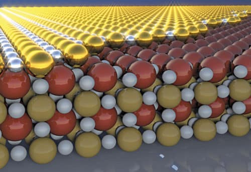
Companies are investing big in exotic forms of carbon as a way to recraft chips. Graphene, for example, is a sheet of carbon atoms just a single atomic layer thick, arranged in a hexagonal array that looks like a chickenwire fencing. Another is carbon nanotubes, which are like tiny straws made from rolled up graphene sheets.
Both forms of carbon could help push miniaturisation further than what’s possible with conventional silicon. And processors could get faster even if they don’t get smaller—a big selling point. Nanotubes could become transistor building blocks, although placing them precisely is a big challenge. Researchers also envision tiny transistors made using graphene, but graphene-based chips will pose challenges. The material conducts electrical current well but doesn’t mirror silicon’s semiconductor properties.

One way to keep pushing progress will involve elements drawn from other columns to either side of the group IV column—thus the term III-V materials, pronounced simply ‘three-five.’ With III-V materials, chip manufacturing stays the same but silicon will get new elements layered on top. That will help electrons flow faster, which means less voltage will be needed to get them moving. If the chips need less power, transistors can be smaller and switch faster.
Researchers are creating and investigating artificial and unconventional materials with unusual electronic and magnetic properties like superconductors that transport electricity with zero losses, and very thin materials (just two or three atoms thick) that could be incorporated into transistors.
The novelty of such materials makes it nearly impossible to anticipate everything that they can do. A researcher can make educated guesses about various properties, but end up seeing something entirely different. A deeper understanding of the material opens the possibility that engineers would be able to route electric currents in quantum computers much like the way they do in conventional electronics through silicon. However, creating high-quality topological insulator materials is a challenge. Since the useful properties occur on the surface, nanoscale ribbons and plates would be ideal to work with because of their large surface area.
British researchers won the 2016 Nobel Prize in Physics for their theoretical explanations of strange states (topological phases) of matter in two-dimensional materials. Their work laid the foundation for predicting and explaining bizarre behaviours that experimentalists discovered at the surfaces of materials, and inside extremely thin layers. These include superconductivity—the ability to conduct electricity without resistance—and magnetism in very thin materials.
Physicists are now exploring similar states of matter for potential use in a new generation of electronics including quantum computers. And the theories pioneered by the Nobel winners have been extended to develop exciting materials such as topological insulators.
Topological insulators
Topological insulators are a class of solids that conduct electricity like a metal across their surface but at the same time block the current’s flow like a rubber through their interior. Theoretical physicists predicted their existence in 2006 and experimentalists demonstrated the first such material in 2008.
Engineers find a few traits of topological insulators especially exciting. One is that the electrons move in a direction determined by their spin—a quantum-mechanical property that forms the basis of magnetic data storage. Engineers hope to exploit the spin-motion connection to make superfast hard drives.
Topological insulators open the door to tailoring topological electronic properties by stacking different thin sheets, or 2D materials. These exotic 2D materials could be used as a platform for energy-efficient computing (spintronics) and to solve today’s intractable challenges with quantum computing.
Candidate materials for topological insulators
Tungsten ditelluride
Like graphene, the semi-metal tungsten ditelluride (WTe2) can be prepared in a single monolayer. Tellurium atoms sandwich the transition metal tungsten in each layer. These sandwiched transition metal materials are important for future electronics and photonics. Scientists have predicted that WTe2 in monolayer form has the exotic electronic properties of topological insulators. However, the surface of WTe2 oxidises in air, destroying the electronic properties.
Now, researchers have made devices from WTe2 down to a single layer thick, which are air-stable and have good electrical contacts. Surprisingly, they found that in the case of a single layer, the sheet became insulating at liquid nitrogen temperatures when no gate voltage was applied. For large-enough positive or negative contact voltages, the electrical current switched on, as in a transistor.Most remarkably though, the insulating state was not fully insulating—it still conducted at the edges. Multi-contact electrical transport measurements and scanning probe techniques verified this conductivity at the edge. This edge conduction is just what is expected for a 2D topological insulator. It exhibits another topological signature in its electronic spectrum—electron states at all energies, without the gap normally found in semiconductors and insulators. The special edge conductivity is sensitive to a magnetic field pointing parallel to the layer.
These observations are consistent with the edge conduction channels behaving like quantum mechanical wires in which the electron magnetic direction, known as spin, is locked to the direction of electron travel. Therefore the edge of the material can be used to filter electrons by spin direction.
The only previous 2D topological insulator candidates were quantum wells in sophisticated semiconductor heterostructures. Likewise, this 2D material can readily be combined with layers of superconducting and magnetic materials. It may thus provide the basis of a platform for spin-based or topologically protected quantum computing.
Transition metal oxides (TMOs)
These are a class of materials that share a common crystal structure known as perovskite. They consist of oxygen and a transition metal element such as copper, iron, manganese, cobalt or titanium. The objective is to preserve the perovskite structure while swapping out different transition metal elements to create materials with a range of electronic and magnetic properties, including superconductivity, ferromagnetism and large thermopower. TMOs are useful in a range of applications from electronics to power transmission to refrigeration.
In an attempt to help scale down the size of electronic devices to atomic dimensions, researchers have demonstrated how to convert a particular transition metal oxide from a metal to an insulator by reducing its size to less than one nanometre thick. The study authors explain how they were able to synthesise atomically thin samples of lanthanum nickelate (LaNiO3) utilising a precise growth technique known as molecular-beam epitaxy (MBE).
Researchers discovered that the process caused the material to abruptly change from metal to an insulator when its thickness was reduced to less than one nanometre. Following that change, the conductivity switched off, preventing electrons to flow through the material—a trait which could be beneficial for use in nanoscale switches or transistors.
Using a unique system that integrates the growth of MBE film with a method known as angle-resolved photoemission spectroscopy, researchers detailed how the specific movements and interactions of electrons in the material were altered, thus changing the thickness of their oxide films on an atom-by-atom basis. They found that once the films were less than three nickel atoms thick, electrons formed an unorthodox nanoscale pattern similar to that of a checkerboard. The discovery demonstrates the ability to control exotic transition metal oxides’ electronic properties at the nanometre scale, while also revealing the surprisingly cooperative interactions that rule electron behaviour in these types of extremely thin substances.
The authors report that their work helps pave the way for use of oxides in the creation of next-generation electronic devices. They wrote that these transition metal oxides have several advantages over conventional semiconductors, including the fact that their high carrier densities and short electronic length scales are desirable for miniaturisation, and that the strong interactions open new avenues for engineering emergent properties.
Bismuth compounds
These have become researchers’ topological insulators of choice as they are simple and economical to make. Chemists in China have precisely grown arrays of ultra-thin flakes of bismuth selenide and bismuth telluride on a surface.
These bismuth compounds, researchers think, promise a new realm of fast, energy-efficient electronic devices and computers. Making well-defined nanoparticle arrays is a key step toward such devices. Growing uniform bismuth-based topological insulators at well-defined spots might be a step towards spin-based electronic devices that would perform computer logic using spin rather than electron charge to represent information, leading to faster, more energy-efficient computers.
Samarium hexaboride
An odd and iridescent material called samarium hexaboride is also classified as a topological insulator. What makes samarium hexaboride unusual is that while it imbibes two distinct properties, its chemical composition remains the same throughout.
Researchers used a technique known as torque magnetometry to come up with first direct evidence to prove that samarium hexaboride is a topological insulator, observing oscillations in how the material responded to a magnetic field. Their technique also revealed that samarium hexaboride contains Dirac electrons on its surface. Because samarium hexaboride is a strongly correlated material, its electrons engage more closely with each other than in most solids, giving its interior electricity-blocking capabilities.
Spintronics uses electron spin at nanoscale to enable nanoscale magnetic sensors as well as advanced magnetic memories. Yet, researchers have not yet attempted to exploit new and exotic magnetic materials like (classical and quantum) spin ice—materials in which electron spin and orbital motion combine to produce very unusual effects such as magnetic monopoles and artificial photons.
Researchers have pioneered the physics and materials science of spin ice, recently creating the first atomic-scale thin films, as well as innovative new approaches to develop the spintronics of spin ice.
The team will investigate how electronic signals can be coupled to exotic magnetism—for example, currents of magnetic monopoles. The aim is to create new spintronic effects and new ways of probing exotic magnetism and how monopoles couple to electron-spins and photons using recently-developed spintronic probes. The successful application of spintronics to spin-ice thin films will start a new chapter in low-temperature condensed-matter physics and practical spintronics.