“Electric floods”, or more precisely, “charge floods”, are a prominent concern to the chip manufacturers today. Electric charge is fundamental in the nature around us. A mere rubbing of two suitable materials is enough to demonstrate these charges. A typical human body may become a storehouse of sufficient charge just by a casual stroll across the carpet. And since the nature loves to restore its balance back, one may experience a minor shock when touching the door knob or the metal cupboard thereafter. This is effectively due to the rapid flow of accumulated charge from the body back to the ground. While the human body is unaffected by such minor shocks, these shocks may contain enough charge beyond a typical IC’s capacity. When forced with such a rapid charge flow, the delicate chip can be easily collapse. Such a collapse is called an ESD (Electro static Discharge) failure, and is similar to the destruction a large rapid flood effects an unguarded city. In the worst case, it may lead the chip and the entire sub-system ineffective, causing significant losses. The concern rises in applications where the chip may be in proximity with high voltage devices, like industrial communications.
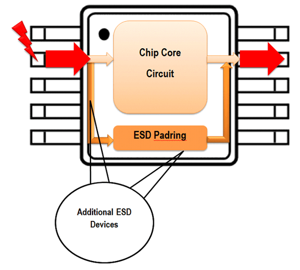
Chip manufacturers hence like to make their chip “flood-proof” by classifying these failures and including several guard mechanisms. A typical chip may in fact contain as much as 10% of its area dedicated to such guard mechanisms, typically called the ESD pad ring. To understand this protection mechanism, it is instructive to reflect back upon the analogy of a flood in the city. A flood prone but properly planned city, apart from the core residential and working areas, may also include a flood dam and flood gates to distract the undesired water away. While they would be shut off during normal operation of the city, they would prove vital in case of emergent floods. For the chip or a board, these flood gates are designed to open automatically as soon as an undesirable quantity of electric charge is seen to be coming into the core. A typical mechanism for such protection would be to divert the entire charge to a central pool, from where it can find its way out through some other pin. The mechanism is incorporated using the ESD Pad ring. This additional circuitry consists of several protection circuits. For instance, all IO pins are equipped with diode based “valves” for diverting any excess charge on pins to supplies. The supplies are further equipped with ESD clamps to protect internal circuitry from over voltages. These clamps help connect to the pad ring core as well, and operate during abnormal conditions. Since all pins will connect to some supply in a circuit, the pad ring will hence also have a connection to every other pin. An exhaustive net is hence activated during an ESD event that can connect every required pin to other pins to drain away the excess charge. The chip, overall, acts as if short-circuited or bypassed by the pad ring.
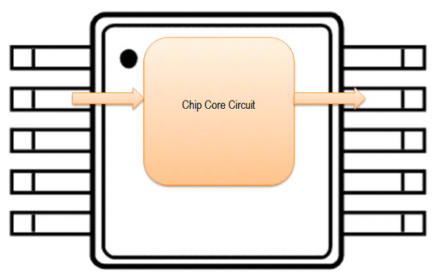
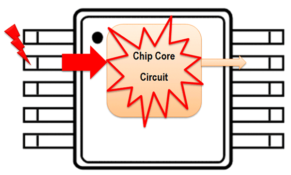
However, care must be taken that a normal flow is not calculated as an overflow, and that the automatic security can well differentiate the two. Since all of this must be done irrespective of whether the chip is activated or not, the design difficulty takes an entirely new level. Figures 1-3 demonstrate the concept more graphically.


The semiconductor industry typically classifies these “floods” into 4 types, depending upon their nature and the magnitude. A human touch to the chip may induce a static ESD discharge best emulated by the Human Body Model, or HBM. A machine touch, on the other hand, due to its metallic character, is best modeled by Charged Device Model (CDM) and Machine Model (MM), depending upon the requirements. A powered device touching an unpowered device would introduce the most aggressive charge flood, typically standardized as the IEC 61000-4-2 standard. There are also other standards like Human Machine Model (HMM), but are less popular. Manufacturers typically qualify to one or more of these standards to rate their products’ strength against ESD failures, depending upon application. For instance, an RS-485/422 compliant communication transceiver chip may be available with a stress qualification as high as ±15,000 Volt HBM owing to the voltages it needs to forbear. Depending upon the other applications, these ESD qualifications vary among chips.
ESD mechanisms can be effective on chip, but the modern call for more and more features pushes the boundaries of chip design. This aggravates the problem for an ESD designer since more effective means more guarding must be employed. This is an area of active and ongoing research and innovation.


