


A central theme in nanotechnology, quantum dots can tune their band gap, which enables these to control the frequency of light emission and absorbance.
Quantum dots (QDs) are semiconducting particles that are a few nanometres in size. Due to their small size, these can confine electrons’ motions. These have the ability to tune their band gap, which enables these to control the frequency of light emission and absorbance. After absorbing a photon of light, these emit a photon of longer wavelength.

Wavelength of the emitted photon can be controlled by controlling the size of QDs. Hence, it is possible to control their properties (electrical and optical) according to their use.
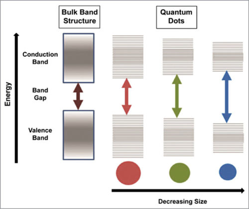
A full range of QDs can be manufactured, each with a narrow, distinct emission spectrum by manipulating the colour of light emitted from these. QDs emit light of a particular colour after being illuminated by light. The colour depends on the size of the nanoparticle, that is, difference between conduction band (CB) and valence band (VB). The smaller the nanoparticle, the larger the difference between CB and VB, resulting in a deeper blue colour. For a larger nanoparticle, the difference between CB and VB is lower, which shifts the glow towards red.
Recently, a NASA technologist has teamed with the inventor of a new nanotechnology that could transform the way space scientists build spectrometers. It is an important device used by all scientific disciplines to measure the properties of light emanating from astronomical objects, including Earth.
Absorption spectrometers measure absorption of light as a function of frequency or wavelength due to its interaction with a sample, such as atmospheric gases. This technology allows instrument developers to generate nearly an unlimited number of different dots, and have precise control over what each dot absorbs. It helps them customise instruments to observe many different bands with high-spectral resolution. This emerging technology could give scientists a more flexible, cost-effective approach for developing spectrometers.
Working of QD technology
When an electron absorbs a photon, it rises to CB from VB. In doing so it leaves a hole in VB, the electron and hole pair together called exciton. Average distance between the electron and hole is known as Bohr Radius. When the size of the semiconductor reduces in comparison to Bohr Radius, it is called QD. After a certain time period, the electron falls back to VB and combines with the hole. This recombination process releases a photon of frequency that depends on band gap energy.
As the size of the crystal decreases, band gap increases. The greater the difference in the energy between highest VB and lowest CB, the more the energy required to excite the dot and, simultaneously, the more the energy released when the crystal returns to VB. This results in higher frequencies of light emitted after excitation of the dot. QDs can be engineered to fluorescence in different wavelengths based on their physical dimensions.
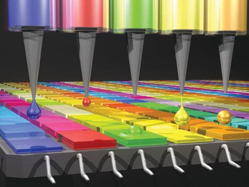
Synthesis of QDs
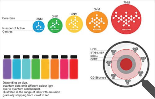
In QDs, electrons are confined in all three dimensions, but there are also other quantum-confined semiconductors. Quantum wires confine electrons and holes in two dimensions, while the third dimension is free to propagate. Quantum wells confine electrons or holes in one dimension and allow free propagation in the other two dimensions. Many semiconductor substances can be used as QDs, such as cadmium-selenide, cadmium-sulfide or indium-arsenide.
Synthesis of QDs require a combination of an appropriate metallic, or an organo-metallic precursor such as zinc, with a corresponding chalcogen precursor such as sulphur. The solvent must be stable at high temperature to prevent particle aggregation. Also, it must act as a surfactant molecule for the stabilisation of QD surface.
Hossam Haick, head – Laboratory for Nanomaterial-Based Devices, Department of Chemical Engineering at Russell Berrie Nanotechnology Institute, explains, “QDs must be produced in an inert atmosphere due to their reactivity. To protect QDs, selection of ligands depends on the desired application of QDs and their dispersion media.”
He adds, “Different methods to stabilise luminescence properties of semiconductor QDs in aqueous media include surface preservation with protective layers, such as proteins and coating of QDs with silicon oxide films, polymer films and so on.”
Sensing and imaging with QDs
Upon heating, QDs undergo significant changes in both luminescence intensity and peak position for a short period. And QD device luminescence in density gradually decreases. Corresponding change in colour is also seen with rise in subsequent temperature.
Optical properties of QDs are related to their size and composition. For biological applications, tuning of optical properties is important. Colour of QDs can be used as a diagnostic tool for sensing applications, to integrate QDs and drug molecules into nanoparticle formulation, conjugate or link drug molecules to QD surface.
Applications of QD technology
Dr Manish Kumar Gupta, assistant professor, Symbiosis University of Applied Science, says, “QDs technology can be used for a wide range of applications such as QLEDs, medical imaging, disease diagnostic, solar cells and photovoltaics, defence, memory devices (quantum computing), humidity and pressure sensors.”
Some common applications of QDs are discussed below.
- QDs are used to detect the presence of biomolecules. For example, these can detect the presence of sugar maltose by conjugating the maltose-binding protein with the nanocrystal surface.
- QDs can also be used for sensing specific DNA sequences.
- High resistance to metabolic degradation and fluorescence properties enable a wide range of experiments.
- QDs’ high photostability and brightness make these suitable for high-sensitivity applications like leaf cell imaging.
- Temperature-dependent changes in optical properties of QDs is the basis for temperature measurement technique.
- Because of their highly-tunable properties, there are various potential applications in transistors, solar cells, LEDs, diode lasers, second-harmonic generation, quantum computing and medical imaging, among others.
- QDs generate two electrons for a single photon of light, as compared to normal solar cells that generate only one electron. Therefore use of QDs increases the efficiency of solar cells in producing electric power.
- QDs display consume less power than current displays. So these are a better choice for applications ranging from cellphones to large-screen TVs.
QDs versus other technologies
The use and application of QDs have many advantages. These require a small amount of energy for excitation regardless of size. This can be achieved by a single blue or ultraviolet wavelength beam. It reduces cost of sensing, too.
Being nanometre in size, QDs have a higher density of states than high-dimensional structures. This means electrons do not have to travel as far as with larger particles. Thus, electronic devices can operate faster.
S.K. Abdul Moyez, research scientist, University of Calcutta, says, “Application of QDs technology is growing widely from semiconducting engineering—including photovoltaic technology, display technology, mobiles and laptops, modern printing technology including ink-jet printing and 3D printing, electrical fields and ceramic engineering—to ultramodern space research technology and cancer therapeutic technology due to their customisable band gap energy and high surface-to-volume ratio.”
QDs are brighter and have little degradation over time, making these superior to traditional organic dyes used in biomedical applications. QD light has a sharp and narrow emission peak, due to a radiative recombination of an exciton. High peak brightness results in a large difference between the bright and dark parts of an image. This property makes QDs suitable for high dynamic range (HDR) displays.
Challenges with QD technology
Manufacturing of QDs is much more expensive than conventional LCDs. However, QDs are still cheaper than OLED displays. And with mass production, QDs display production will soon gain enough efficiencies to become relatively inexpensive.
QD particles are affected by water, heat and humidity, and require isolation. To protect QDs from decomposition due to humidity, a barrier film is currently used as an isolating layer.
Dr Mahesh Sharma, senior scientist, National Physics Laboratory, says, “The first challenge in QDs research is their mono-dispersivity. The other is stability. When kept for a long time, QDs can aggregate and form large clusters. To stabilise, ligands or any surface passivation must be used. This also sometimes interferes in certain desired properties. Photocatalysis and water splitting are some challenging applications.”
Dr Gupta adds, “Existence of free charge carriers and electric fields in LEDs presents a challenge for optimisation of QD band structure. Another big challenge for this technology is on-chip design, as it is hard to achieve. Manufacturing processes have reported challenges in the field of quantum displays, such as low quantum efficiency and need for an in-cell polariser.”
Moyez adds, “Use of toxic but efficient materials in QDs is another factor to be considered for the sake of a green environment. QD polymer complex mixture is hard to develop. QDs in photovoltaic technology may create an excess recombination state, which could lower overall performance. The large size of QDs compared to biological cells is another factor that needs to be overcome.”
Future of QD technology
The future of QD technology depends on the requirement of new applications and development areas. QDs are considered zero dimensional and, hence, exhibit sharper density of states in comparison with structures of higher dimensions. These result in excellent optical as well as transport properties. These properties are currently being studied for potential applications in electronic amplifiers, biological sensors and diode lasers.
Applications and usefulness of QDs technology continue to expand. Researchers are striving to bring the benefits of this technology to more technologically-applied fields. The broad range of real-time applications of QDs technology in the field of medical science is expected to be very useful in disciplines such as lymphocyte immunology, cancer metastasis, stem cell therapeutics and embryogenesis.
Development of QDs will change the face of upcoming technologies. Proper development or commercialisation of QDs in optical and semiconducting fields have already started due to the tunable band gap of QD materials. And more research in sectors such as science, engineering, technology and medicine is essential for a better future.