


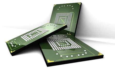
Flash memories have been around for a decade in all sorts of embedded systems. These are used both as code space and non-volatile memory to save data across power cycles.
As we utilise flash to store the configuration data and history records, it is important to predict the lifespan of the product and the number of saves to flash per day in the emerging consumer electronics applications. Though many devices claim a higher number of write cycles, they may be hard-pressed to meet the operating conditions.
Another important concern is the time to write and erase on a memory block. Allen Pothoof, senior software engineer from Esterline Avista, shares, “Erase/write time is important because if you haven’t planned for it, your application may come to a screeching halt while you update some data.”

Flash memory vendors are competing against each other not on process-technology but application-specific solutions to meet the demand coming from emerging consumer applications like tablet PCs, mobile phones, solid-state storage devices, audio players and television sets with digital recording function. for all these devices, to make full use of the benefits offered by flash memories, it is necessary to understand how to rewrite on them.
Flash penetration in embedded apps
There are different types of flash memories available in the market. The type of embedded application determines the type of flash memory that needs to be utilised—while some flash memory companies may be targetting the data storage flash used in applications like SSDs and memory cards, others target a different type of flash used in applications like smart meters, networking equipment, DVD players and Bluetooth products in addition to smartphones and tablet PCs.
Leonid Rosenboim, embedded systems entrepreneur and founder of Certarete, informs, “Initially, flash was used as a replacement for the ultraviolet erasable programmable read-only memory (UV EPROM), mainly to store the program code and data. Some systems used the EPROM/flash in ‘execute in place’ mode to save the RAM, while others copied the code to the RAM to gain a higher execution speed.”
Gradually, “flash grew to replace the electrically erasable programmable read-only memory (EEPROM) by utilising its ability to be modified ‘in-circuit’ and store non-volatile modified ata (such as configuration). Later, more sophisticated embedded systems deployed one of several file system technologies (either fast file system or flash transition layer) to store larger portions of data and program code that was easier to modify (upgrade) in these file systems,” says Rosenboim.
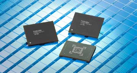
More recently, the file system portion has been increasingly taking advantage of the cost-effective NAND technology. NAND is being used for data storage in addition to OS/apps storage for the applications processor. Richard De Caro, director of strategic marketing for Atmel’s memory business unit, says, “In these cases, portions of the NAND flash are shadowed into the DRAM and the code executed out of the DRAM and not the NAND flash. Standard NAND flash does not provide fast random-access read that is needed for code execution. However, NOR flash is still used in most mobile phone designs as the code-execution flash for the baseband processor.”
[stextbox id=”info” caption=”Open NAND Flash Interface (ONFI) Working Group”]
The Open NAND Flash Interface is an industry working group made up of more than 80 companies that build, design-in or enable NAND flash memory. The group is dedicated to simplifying NAND flash integration into consumer electronics products, computing platforms and any other application that requires solidstate mass storage. They define standardised component-level interface specifications as well as connector and module form factor specifications for NAND flash.
The ONFI Working Group was formed in May 2006 and currently has more than a hundred member companies. ONFI’s founding companies include Hynix Semiconductor, Intel, Micron, Phison, SanDisk, Sony and Spanion.
[/stextbox]
Another interesting trend is that many microcontrollers and even some field-programmable arrays (FPGAs) are now made with embedded flash memory to decrease the component count and cost of embedded systems. All the microcontrollers use an internal, on-chip flash memory for data storage. Embedded flash platforms are also being used for programmable device and systems-on-chip development.
