This is not a ‘frog turned into a prince’ story, but a very long quest by technologists.
Technologists and, yes, advertisers, started dreaming about printed and flexible electronics decades ago, as early as 1970s. Products they wanted to develop evolved over time, but the core requirement of such printed electronics remained the key. The quest for large and flexible banners that could deliver interactive ads, and tablecloths that could be computer displays, evolved into the search for phones that could be folded up like handkerchiefs and flexible digital watches that would cling to your wrists. This continues to grow into more complex goals like flexible body implants and printable human tissues.
What makes today different from 1970s, however, is that dreams are seasoned with reality now. With several commercial products, demonstrations and promising researches, it is evident that printed, flexible and even organic electronics are fast becoming a rampant reality.
Research in this area predominantly classifies under manufacturing methods and processes, both lab-scale and large-scale, materials for substrates and inks, as well as designs. In this story, let us take a look at some such interesting projects transpiring at universities and other research and development (R&D) centres across the world.

Printed spacecrafts and atmospheric confetti
How small would space centres become if spacecrafts could be printed? Well, we would know soon enough. NASA’s Jet Propulsion Laboratory (JPL) has been exploring the idea of designing and fabricating a spacecraft entirely with flexible substrate printed electronics. The idea is to print a two-dimensional sheet with all the functional subsystems of a typical spacecraft, right from measurements to communications.
At the end of the project’s first phase, the team reports, “Atmospheric confetti. Inchworm crawlers. Blankets of ground-penetrating radars. These are some of the unique mission concepts that could be enabled by a printable spacecraft.” The low mass, volume and cost of printed spacecrafts makes NASA believe that, network missions would transform from a few discrete measurements to millions of platforms, achieving greater areal density and system reliability. Printed platforms could be released not just into space but also into volcanic plumes to measure composition and impact energies. These could be fitted in smart solar sails or areal balloons to monitor erstwhile unreachable areas and parameters.
The final report of the project’s second phase affirms that, it is feasible to build an entire spacecraft out of printed electronics, but it raises doubts about launching such a spacecraft off a rocket and having it orient and propel itself to the intended destination. In the near term, applications might be simpler, such as sensors.
Printing power, literally
Last year, California based Imprint Energy demonstrated the print manufacturing of ultra-thin, flexible and rechargeable batteries. This was part of a larger project by FlexTech Alliance to show that multiple key components, such as power source, display and other electronics, can be incorporated onto a flexible substrate to produce a product.
Imprint’s printed ZincPoly 60mWh rechargeable battery powered all components, including the wireless communication module of a wrist-worn device that conforms to a minimum 25mm bend radius, which is considered to be the typical bend radii for wrist-worn wearable electronics. While developing the printed power source, Imprint worked towards multiple technical goals including the ability to scale the manufacturing process, increase single-cell discharge capacity and rate capability, develop flexibility test protocols and equipment, and so on.
Printed electronics is also expected to be very helpful in the printing of flexible solar panels, which can power not just small devices but even cars.
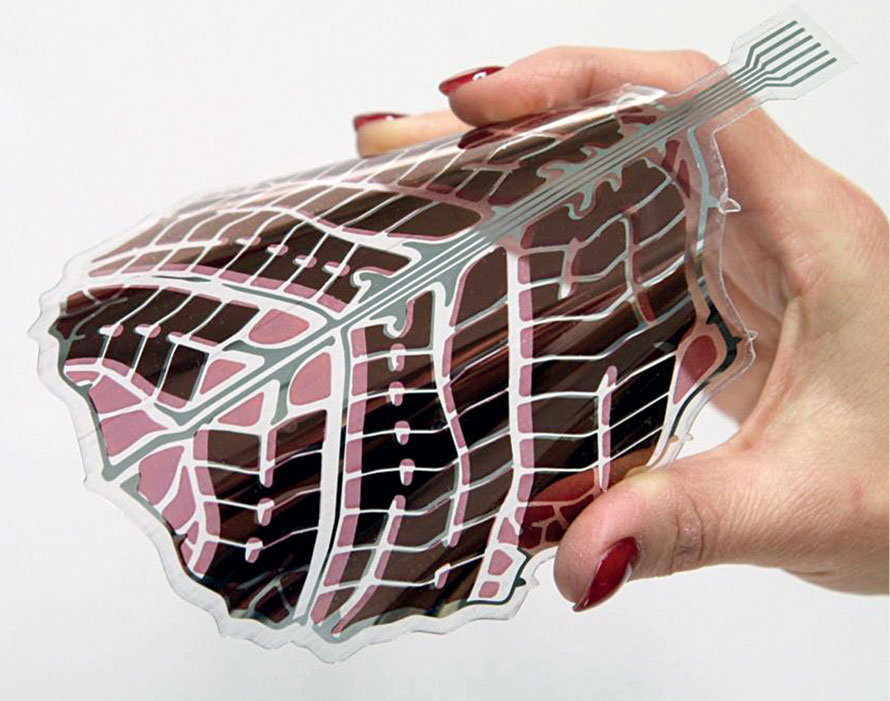
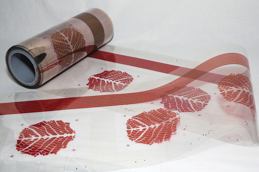
One interesting research in this space is the development of a mass production method for printing decorative, organic solar panels by VTT Technical Research Centre of Finland Ltd. So far, it has been possible to pattern organic photovoltaic (OPV) panels only into strips, but this new method offers complete design freedom, so that panels can be used on surfaces of not just small, decorative objects but also large areas like cars or even exteriors of buildings.
The new solar panels, printed with VTT’s gravure and screen-printing technologies are only around 0.2mm thick and include electrodes and polymer layers, where the light is collected. Graphics can be printed to make the solar panels decorative too. Each leaf printed as a feasibility test has an active surface of 0.0144m2. These include connections and a decorative part. One square-metre of an active solar panel surface comprising approximately 200 OPV leaves generated 3.2 amperes of electricity with 10.4 watts of power at Mediterranean latitudes, where it was tested.
Although efficiency of organic solar panels is lower than traditional silicon based ones, these are more flexible, light, affordable and recyclable, which justifies the growing market for this segment.
VTT is also developing roll-to-roll manufacturing methods for inorganic perovskite solar panels. Performance of a perovskite solar cell is approximately five times better than that of an OPV cell, while material costs are almost ten times lower. That is not all; the research organisation is also exploring how such solar panels can be used as data receivers for wireless communication. Now, that would be a wonderful combination!

Chock-full of energy
Last year, Linköping University, Sweden, started work on a project funded by Swedish Energy Agency to develop integrated energy storage modules in printed electronics. In a span of four years, the team hopes to not only prove that this integration is possible but also that it can be scaled up and manufactured on an industrial scale. One of the perceived applications is economical battery packs for vehicles.
Currently, energy storage in batteries and supercapacitors is done with expensive and complex energy storage cells. It is difficult to distribute electrical energy properly between energy-storage molecules, and balancing circuits are required to monitor the modules and balance these to avoid overload and short circuiting. Connections between balancing circuits and individual cells are also very costly.
Hence, Modulit project aims to develop monolithic integrated energy-storage modules and balancing circuits on polymer. This can be compared to how millions of components are integrated on a single chip in traditional electronics. The team also hopes that the revolution this project will create in the battery and supercapacitor industry will be akin to the revolution created by integrated circuits in the electronics industry.
There is, however, a long way to go, as commercial-scale production of such integrated energy-storage modules will require development of new supercapacitor materials and new electrode materials that can be managed in air and printable balancing electronics.
Best of both worlds
Benefits of flexible, printed sensors are well-known, especially for solutions like smartlabels and wearable electronics. Such solutions require a range of functionality, from complementary logic, power sources, displays and memory devices to the integration of a wide variety of sensor types. While much of this can be achieved through direct, additive printing of solution based inks, some complex computational functionality such as high-resolution analogue-to-digital conversion and wireless communication are better done with conventional silicon based electronics, today.
While this is bound to change in the future as capabilities of printed electronics improve, today it becomes necessary to combine the benefits of printed, flexible, distributed sensors and the performance of silicon electronics, if we want to achieve the best efficiency in some applications. In order to achieve this, Xerox PARC, an expert in large-scale, flexible sensor systems, has come up with a hybrid fabrication platform.
Presented at Nano Bio Manufacturing Consortium (NBMC) Wearable Electronics Workshop last year, this technique allows for printed electronic devices to be used alongside a minimal set of pre-fabricated microelectronic components. By describing how to mechanically and electrically interface printed and microelectronic components in a system that wirelessly transmits data from printed light and temperature sensors, researchers showed that it is possible to combine small, low-profile integrated circuits (ICs) into flexible, custom, high-performance sense-and-transmit systems without affecting the mechanical flexibility of the final system.
Mass manufacture of classic designs
If only it was possible to mass-print device designs, it would mean a great relief for numerous electronics engineers stumped with how to take their printed electronics research out of the lab into large-scale production.
One step towards this was taken by PARC and Clemson University last year in a project facilitated by FlexTech Alliance. The project explored how to scale up and print functional devices on a commercial printing press.
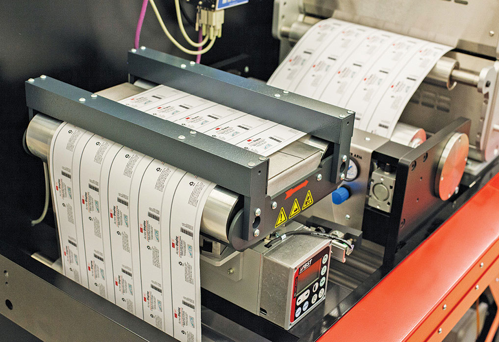
PARC contributed brilliant device designs amenable to inkjet printing, which it generally printed using a lab-scale gravure printing press not suitable for high-speed, roll-to-roll throughput. Clemson University came into the picture with its seven-station Omet printing press, a modular platform. The goal of the project was to achieve multi-layer device printing with a gravure or flexo-hybrid approach.

This involved several customisations to the press, inks and design. For starters, the team engineered a chambered doctor blade system on Omet press. The chamber enables users to seal a small volume of ink, less than 50ml, against the cylinder, unlike normal gravure press configurations that use a large amount of ink to fill the pan. This restricts ink usage, saving money in the bargain.
A variety of inks were tested, and numerous functional multi-layer devices such as capacitors, diodes and thin-film field-effect transistors (FETs) were printed. Device parameters were optimised using high-speed optical metrology, and resistivity of around 4X bulk silver for features approximately 50nm thick at speeds of around 60m/min (200-feet/minute) were achieved, with very high yield.
Up in 2016: Printed sensors to watch engines and motors
University of California at Berkeley and California Polytechnic State University in San Luis Obispo, both in the USA, are working towards developing fully-integrated, printed, self-rechargeable wireless sensor nodes for engine and motor condition monitoring.
Condition based monitoring (CBM) is in great demand today and is required by most industries. The advantage of using flexible electronics for this purpose is that, devices can be designed to fit unique geometries. In this case, the team plans to use a flexible substrate, so that the device can be rolled up into a cylinder with a small footprint. This will be a big jump from the use of bulky and heavy equipment that cannot be integrated into the limited space around engines and motors. By using multiple printing methods like flexographic, dispenser and screen printing, the team hopes to produce a proof-of-concept device by early 2016.
This unique device will harvest and store energy from the waste heat of the engine to keep sensors running for much longer than traditional sensor nodes. It will have a printed thermoelectric generator for generating power from engine waste heat, printed supercapacitor for supplying sufficient duty-cycle power, printed battery for storing harvested energy and long-term power, and an accelerometer for sensing the engine’s vibrations to keep a tab on its health.
Ink matters
Ink is another major area of innovation in the world of printed and flexible electronics. One such example is a project at Acreo Swedish ICT to develop ink that can print electronics for different applications, which can be used any time, come rain or shine.
When developing electrochemical components, the key component is electrolyte. If you take the example of traditional batteries or electrolytic condensers, the electrolyte is hermetically sealed in a metal casing. However, when you take the example of a printed display, the electrochemical cell has to function without hermetic encapsulation in all kinds of environments. Additionally, the material must also be non-hazardous, right from manufacture and handling to disposal.
There are other requirements also that electronic ink must meet. It must not dry in the press but must dry quickly once deposited on the substrate. It must spread on the surface at just the right speed so that it can be controlled and also forge well with the substrate. It must be durable, pliable and compatible with other materials that might be used in the product.
Acreo is working to develop an ink, based on polyelectrolytes, which will meet all, or at least most, of these expectations. They are also working with Linköping University to study the curing of ink. In a press report, Dr Mats Sandberg of Acreo explained that, systems for ultraviolet (UV) curing used for graphic printing ink are good enough for bonding pigment but it does not work well enough for functional printing ink. “In order for the electronic printing ink to harden rapidly enough, we need to develop new bonding agent chemistry,” he said.
Acreo is working to solve such problems and so are numerous other organisations around the world. Technologists have been working on printed and flexible electronics for a long time now, but it is evident that they are now in a real hurry because there is scope for a number of new applications, which will involve innumerable objects with printed electronics working together with mobile phones and, you guessed it right, the Internet of Things! Indeed, there is a lot of excitement in store for us.


I dont want this email
Kindly elaborate your query.