The need of the hour is higher speed at lower power consumption. A laptop is expected to boot-up quickly and its charge to last for at least a few hours. Military equipment must function right in the most stringent conditions. No one wants to go in search of a particular kind of charger for a mobile just because the one he or she has cannot function on the available alternating current (AC) power line in another country.
These are scenarios we never give a second thought to. But essential parts driving each of these are transistors, transformers and rectifiers put together on or around a chip, coming to the fore as a power supply system. Right from a simple torch to something as complex as a satellite system, power-conversion components play a vital role in their functioning. This article tries to look at the latest developments in this sector of electronics and what makes these improvements kick in.
Moving away from silicon
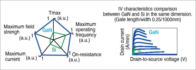
In order to improve system efficiency and lower the form factor, increasing the switching frequency of the system is one viable solution. Critical components for high-frequency action of power-management components are metal oxide semiconductor field-effect transistors (MOSFETs), accompanied by related drivers. Higher the frequency, higher is the required gate charge, and it is common to use MOSFETs in parallel to achieve an effective lower resistance and higher gate charge. But, there is also a need to make sure that switching loss is lower.
Even with all the enhancements in the silicon wafer, power-conversion components ask for more. While going to lower and lower nodes certainly helps achieve higher switching frequencies in the order of GHz, power-related devices demand a MHz range. Thus, there is a shift towards using materials like gallium-nitride (GaN) and silicon-carbide (SiC).
Lower switching loss. GaN and SiC offer a higher band gap as compared to silicon, and thus the system design itself undergoes a change. GaN MOSFETs were, in the past, mainly used in low-voltage applications (<100V). Now, GaN based devices target voltage ranges from 200V to 700V, while SiC based devices target a voltage range above 700V. The first 600V-650V GaN was commercialised by Transphorm & Efficient Power Conversion Corp. (EPC) in 2014, and now companies like Infineon and Texas Instruments (TI) have joined this trend. Started off by Cree, SiC MOSFETs are now being manufactured by Microsemi, STMicroelectronics, Toshiba and Infineon, to name a few.
Gate-charge driver is as important. While the main advantage is that GaN and SiC offer high-frequency support with lower switching loss, and a smaller form factor, driving the gate circuit for these materials requires a negative voltage to be applied, moving away from the traditional silicon based approach. To make it easy to cope with this change, designers are coming up with specialised drivers.
While there have been efforts to provide components and drivers in a single package for easy end use, the design process is complex. Some vendors prefer to separate out the two in order to offer more flexibility in matching existing drivers with transistors of different ratings.
Spanning a range of voltages and temperatures
With power-conversion components present in all kinds of electronic devices/gadgets, it is imperative for these to support a range of temperature and voltage operations.
Components are rated according to grids. Commercial applications are the ones working at least power and temperature ranges, but have to take into account power fluctuations. Ones used under the hood of automobiles and light emitting diodes (LEDs) need to support about 150°C temperature. Reliability and high tolerance are prime deciders for military-grade components, while those that go into space electronics need to withstand many kinds of radiations.
Products that work on AC mains like LED bulbs and inverters take in 220V AC input and convert it to high-range voltages. High voltages demand heavy device capability, and to support these, there are MOSFETs, bipolar transistors and insulated-gate bipolar transistors (IGBTs), competing in the same space.
Traditionally, voltage handling was highest for bipolar technology. With IGBT disrupting this technology, it is now common to find IGBT modules in high-voltage equipment like the uninterrupted power supply (UPS).
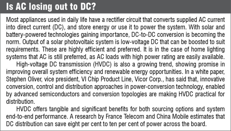
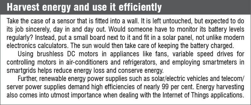
Batteries to the rescue. Battery-powered devices like mobile phones and wearables perform power conversion at direct current (DC) range, and at much lower levels. Battery is expected to charge fast, be stable and reliable. A power supply also needs to tolerate high voltages and not break down in such scenarios. To add to the burden, there is the case of wireless charging.
 Many battery-operated systems use two or more supercapacitors in series. In an earlier interview, Robert L. Chao, founder, Advanced Linear Devices Inc., explained how MOSFET based current balancing is enabling reduced power use in superconductor stacks. He says, “A MOSFET array balances leakage currents in each cell by exponentially varying currents relative to selected operating voltages. This method compensates for leakage-current imbalances with small voltage imbalances so that maximum rated voltage limits are not exceeded.”
Varying models for different end applications
While designing power-conversion components, lifestyle of consumers and application of the system also define scalability of the design. Current-handling capability and failure protection of the designed circuit reflects its complexity, cost and size.
Consider the case of a metering device. Presently, a majority of digital residential meters are non-communicative, with no electronic controlling capabilities. Power requirement for such systems will hardly be 0.5W to 2W. However, futuristic smartmeters look to integrate communication capabilities and remote control facilities within, and this would demand a difference in the design. Thus, system developers design variant models of power-sourcing circuits.
Conquering heat
Small sizes and higher packing densities automatically come with the drawback of higher heat generation. µModule from Linear Technology facilitates sharing of the heat-sink between digital microcontroller circuits and the module.
There is also another trend that is seen. Instead of adding heat-sinks and fans, the industry is trying to use the printed circuit board (PCB) itself to dissipate the heat generated. There are two developments to counter this problem. One is to use a material on the PCB that removes heat, and/or use multi-layer boards, and the other is to adopt multi-purpose packaging technologies.
Packaging plays a vital role. Requirement for reduced package size has resulted in tiny lead-less or ball grid array (BGA) packaging with extremely small pitches. This requires reduced power consumption, leading to reduced voltages. Increases in thermal stresses on chips create a requirement for thermal pads, for effective heat dissipation. Heat from the chip goes into the power pad, from where it is transferred to the surface of the PCB and then dissipated.

Quad Flat No Leads packaging is dominant. TO-XX packaging offers a wide range of small-pin-count packages for discrete parts like transistors or diodes. Smaller the package, higher is the professionalism required to solder the components.
This packaging trend not only satisfies the need to fit in maximum things into minimum space but also takes care of miniscule-size restrictions demanded by peripheral component interconnect express (PCIe) cards and wearable devices.
Making performance count
Optimising the performance of a chip within its limits of cooling, packaging and power supply capabilities is a mighty challenge. While dynamic voltage frequency scaling is one traditional method, MIC95410 7A load switch from Micrel permits power partitioning in systems, and is also capable of controlling power-up sequence using a ramp signal.
A stable and noise-free source. It is also necessary to make sure that operation of a power-sourcing circuit is stable and noise-free. In a sensor based data-acquisition circuit, a slight change in output of the powering circuit can result in large variations in sensor calibration, resulting in erroneous data. Thus, precise voltage regulation of power-sourcing circuits is of prime importance for maintaining system integrity.
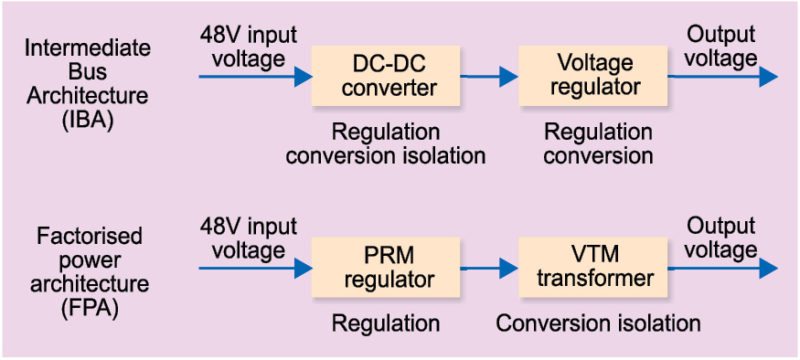
Improving efficiency. Vicor has come up with Factorised Power Architecture (FPA) to solve power-related performance issues. Enabling components are integrated power components called VI Chips. FPA aims at providing the highest degree of system flexibility, power density, conversion efficiency, transient responsiveness, noise performance and field reliability.
Design with caution. Design of the PCB also comes into prominence when inductive components like motors and solenoids are involved. These components tend to create spikes in current, and PCB parts have to be designed with optimum protection to handle this surge. There is also a need to build isolation into these solutions, separating the secondary from the effects of the primary winding of the transformer.

While trends in power-conversion components are not advancing as rapidly as, say, the Internet of Things or infotainment, tried-and-tested new developments are here to stay. Keep on the lookout for more.
Priya Ravindran is a technical journalist at EFY


Excellent information. It increases the little knowledge that I can have in electronics. As time imposes an action limit on the field of electronics, I record and then analyze the information as far as I can and the results are excellent. Thank you for such an important contribution to expand the knowledge of those involved in this technique or profession of high level or just have little knowledge of electronics. My congratulations on that valuable contribution. Rafael Ortega
Thank you for your feedback.